
Cluster-type PVD System with Glovebox [KVE-TG4000L] > Applications
-
제품 정보
제품 상세설명
Overview
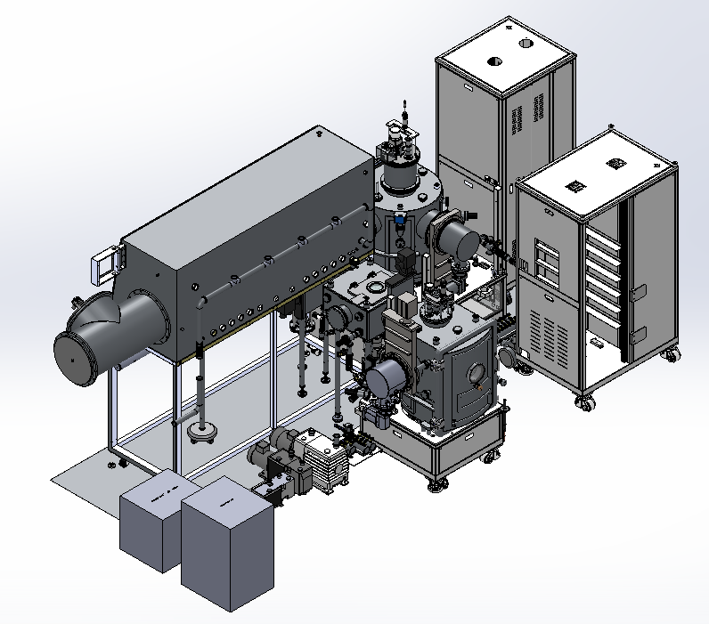
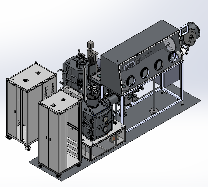
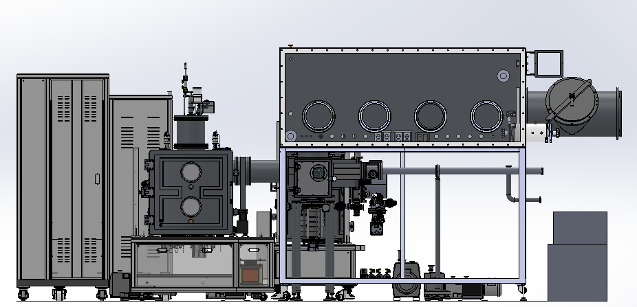
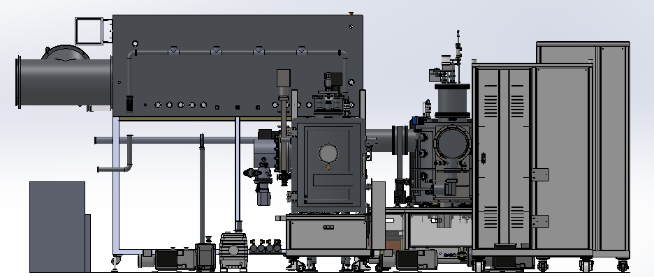
This is a multi-faceted integrated vacuum deposition equipment designed to research, develop, and produce initial prototypes of ultra-small LED chips (each measuring 100 μm or less) that are the core of high-resolution, high-efficiency Micro LED displays. Unlike typical large-scale mass production lines, it features a compact structure optimized for laboratories and pilot lines, while being capable of forming high-quality thin films without contamination between modules.
Features
- Prevention of interfacial contamination through in-situ processes: During electrode deposition after mesa etching or thin film deposition after cleaning, the substrate is transported while maintaining an ultra-high vacuum state without being removed to the atmosphere, thereby completely preventing device performance degradation caused by surface oxidation or moisture adsorption.
- Process Flexibility: The chamber configuration can be modified to suit research and development purposes, or new modules (e.g., cells for organic material deposition) can be added for future expansion.
- Space and Cost Efficiency: Compared to large-scale mass production cluster equipment, it has a smaller footprint, allowing for deployment within limited laboratory space. Furthermore, it is optimized for small-volume wafer processing, enabling reduced running costs.
Overview
This is a multi-faceted integrated vacuum deposition equipment designed to research, develop, and produce initial prototypes of ultra-small LED chips (each measuring 100 μm or less) that are the core of high-resolution, high-efficiency Micro LED displays. Unlike typical large-scale mass production lines, it features a compact structure optimized for laboratories and pilot lines, while being capable of forming high-quality thin films without contamination between modules.
Features
- Prevention of interfacial contamination through in-situ processes: During electrode deposition after mesa etching or thin film deposition after cleaning, the substrate is transported while maintaining an ultra-high vacuum state without being removed to the atmosphere, thereby completely preventing device performance degradation caused by surface oxidation or moisture adsorption.
- Process Flexibility: The chamber configuration can be modified to suit research and development purposes, or new modules (e.g., cells for organic material deposition) can be added for future expansion.
- Space and Cost Efficiency: Compared to large-scale mass production cluster equipment, it has a smaller footprint, allowing for deployment within limited laboratory space. Furthermore, it is optimized for small-volume wafer processing, enabling reduced running costs.
-
Specifications
제품 Specifications
-
Options
제품 Options
Options
- Etc... user requirements
Options
- Etc... user requirements
-
Control
제품 Control
System Control
- Etc... user requirements
System Control
- Etc... user requirements
-
사용후기
-
상품문의
-
배송/교환정보
[배송]
배송 안내 입력전입니다.[교환]
교환/반품 안내 입력전입니다.
선택된 옵션
-
Cluster-type PVD System with Glovebox [KVE-TG4000L]+0원
관련제품
등록된 상품이 없습니다.