Josephson Junction System
-
 By maximizing the unique properties of aluminum, the JDR-E series delivers the ultimate hardware solution for producing top-tier Josephson junctions.
 -
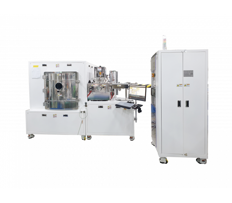
 CLUSTER SPUTTER VACUUM EQUIPMENTS
 -
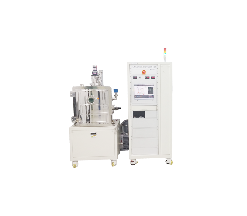 Thermal Indium Series
 -
 By maximizing the unique properties of aluminum, the JDR-E series delivers the ultimate hardware solution for producing top-tier Josephson junctions.
 -
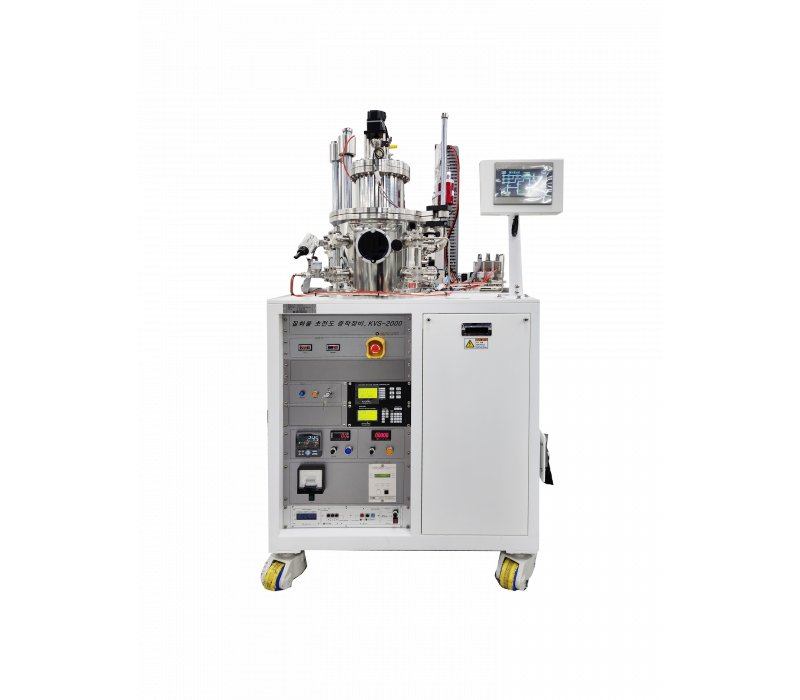 By harnessing the superior stability and higher critical temperature of Niobium, the JDR-S series delivers the ultimate sputtering solution for fabricating highly reliable Josephson junctions.
 -
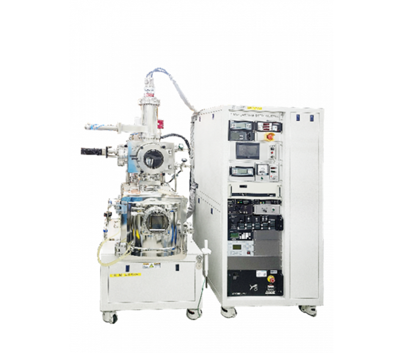
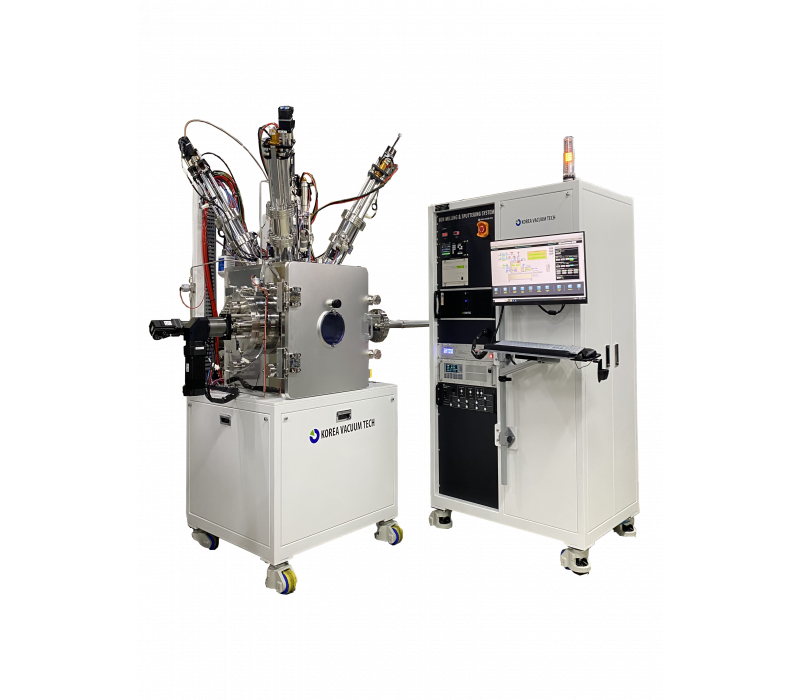
 Ion beam etching is a microfabrication process essential for fabricating Josephson junctions. Josephson junctions, which involve nanometer-thick insulating and superconducting layers, require extreme precision. Ion beam etching selectively removes only unnecessary components, creating a clean and uniform junction surface and optimizing intermetal contact characteristics to ensure stable supercurrent flow. This precision processing technology is a key enabler for high-performance qubit implementation and large-scale quantum chip fabrication.
 -
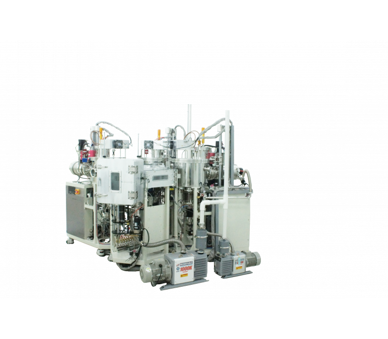
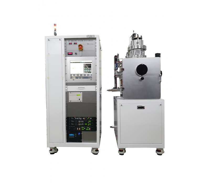
 Josephson junction fabrication requires extreme precision, and ion beam etching and sputtering are key processes for achieving this. Ion beam etching selectively removes unnecessary film to ensure a clean and uniform bonding surface, while sputtering deposits a precise and uniform film of superconducting metals such as neodymium (Nb) or aluminum (Al). Our integrated vacuum system is designed to perform these two processes continuously within a single chamber. Contamination is minimized by eliminating sample exposure to the atmosphere between processes. This system simultaneously meets the stability, precision, and efficiency demands of researchers and industrial sites, providing the optimal solution for the development of next-generation superconducting quantum computers.